- 您现在的位置:买卖IC网 > Sheet目录1905 > ATMEGA3250V-8AI (Atmel)IC AVR MCU 32K 8MHZ 100TQFP
PCA9698
All information provided in this document is subject to legal disclaimers.
NXP B.V. 2010. All rights reserved.
Product data sheet
Rev. 3 — 3 August 2010
28 of 48
NXP Semiconductors
PCA9698
40-bit Fm+ I2C-bus advanced I/O port with RESET, OE and INT
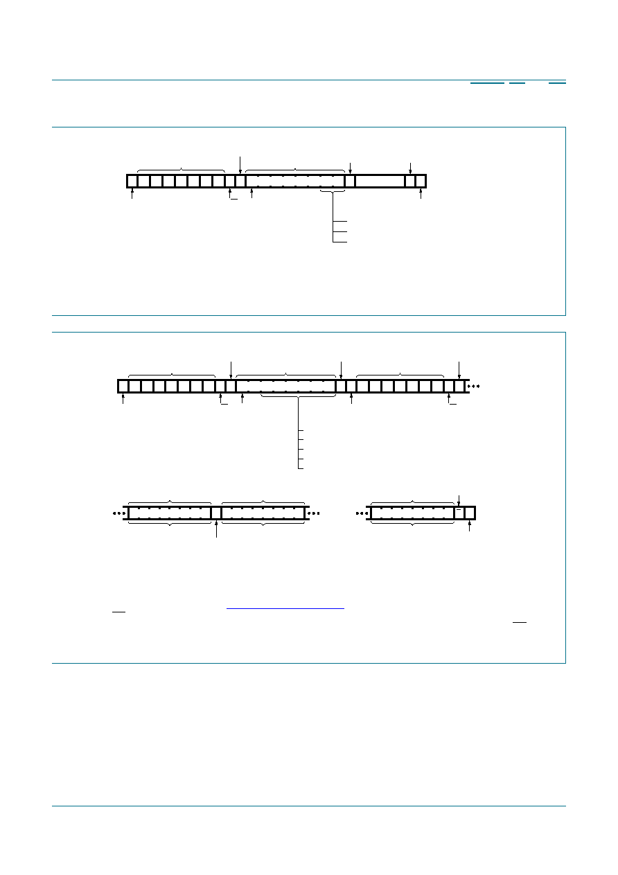
The programming becomes effective at the Acknowledge.
If more than 1 byte is written, previous data is overwritten.
Fig 18. Write to the output structure configuration, all bank control, or mode selection
002aab947
S A6 A5 A4 A3 A2 A1 A0 0 A
slave address
R/W
START condition
command register
AI = 'don't care'
A
acknowledge
from slave
DATA
A
acknowledge
from slave
acknowledge
from slave
P
STOP condition
SDA
X
01010 D1 D0
00 for output structure configuration programming
01 for all bank control register programming
10 for mode selection register programming
If AI = 0, the same register is read during the whole sequence.
If AI = 1, the register value is incremented after each read. When the last register bank is read, it rolls over to the first byte of the
category (see category definition in Section 7.3 “Command register”).
The INT signal is released only when the last register containing an input that changed has been read. For example, when
IO2_4 and IO4_7 change at the same time and an Input Port register read sequence is initiated, starting with IP0, INT is
released after IP4 is read (and not after IP2 is read).
Fig 19. Read from Input Port, Output Port, I/O Configuration, Polarity Inversion, or Mask interrupt registers
002aab948
S A6 A5 A4 A3 A2 A1 A0 0 A
slave address
R/W
START condition
command register
AI = 1
A
acknowledge
from slave
A
no acknowledge
from master
acknowledge
from slave
P
STOP condition
SDA
1
0 D5 D4 D3 D2 D1 D0
Sr
repeated START
condition
A6 A5 A4 A3 A2 A1 A0
slave address
1 A
R/W
acknowledge
from slave
data from register
DATA
A
acknowledge
from master
first byte
register determined
by D4 D3 D2 D1 D0
data from register
DATA
second byte
data from register
DATA
last byte
D[5:0] = 00 1000 for Output Port register bank 0
D[5:0] = 01 0000 for Polarity Inversion register bank 0
D[5:0] = 01 1000 for Configuration register bank 0
D[5:0] = 00 0000 for Input Port register bank 0
D[5:0] = 10 0000 for Mask Interrupt register bank 0
发布紧急采购,3分钟左右您将得到回复。
相关PDF资料
ATMEGA328P-15AZ
MCU AVR 32K FLASH 15MHZ 32-TQFP
ATMEGA32L-8PJ
IC MCU AVR 32K 5V 8MHZ 40-DIP
ATMEGA32M1-AUR
IC MPU AVR 32K 20MHZ 32TQFP
ATMEGA48PA-MMNR
MCU AVR 4KB FLASH 20MHZ 28QFN
ATMEGA644P-B15MZ
IC MCU 8BIT 64KB FLASH 32VQFN
ATMEGA644V-10PU
IC AVR MCU FLASH 64K 40DIP
ATMEGA645V-8MI
IC AVR MCU FLASH 64K 1.8V 64QFN
ATMEGA649-16MI
IC AVR MCU FLASH 64K 5V 64QFN
相关代理商/技术参数
ATMEGA3250V-8AJ
制造商:ATMEL 制造商全称:ATMEL Corporation 功能描述:8-bit Microcontroller with In-System Programmable Flash
ATmega3250V-8AU
功能描述:8位微控制器 -MCU AVR 32K FLASH 1K EE 2K SRAM ADC 1.8V RoHS:否 制造商:Silicon Labs 核心:8051 处理器系列:C8051F39x 数据总线宽度:8 bit 最大时钟频率:50 MHz 程序存储器大小:16 KB 数据 RAM 大小:1 KB 片上 ADC:Yes 工作电源电压:1.8 V to 3.6 V 工作温度范围:- 40 C to + 105 C 封装 / 箱体:QFN-20 安装风格:SMD/SMT
ATMEGA3250V-8AUR
功能描述:8位微控制器 -MCU AVR 32KB FLSH 1KB EE 2KB SRAM-8MHZ 1.8V RoHS:否 制造商:Silicon Labs 核心:8051 处理器系列:C8051F39x 数据总线宽度:8 bit 最大时钟频率:50 MHz 程序存储器大小:16 KB 数据 RAM 大小:1 KB 片上 ADC:Yes 工作电源电压:1.8 V to 3.6 V 工作温度范围:- 40 C to + 105 C 封装 / 箱体:QFN-20 安装风格:SMD/SMT
ATmega325-16AI
功能描述:8位微控制器 -MCU AVR 32K FLASH 1K EE 2K SRAM ADC 5V 5V RoHS:否 制造商:Silicon Labs 核心:8051 处理器系列:C8051F39x 数据总线宽度:8 bit 最大时钟频率:50 MHz 程序存储器大小:16 KB 数据 RAM 大小:1 KB 片上 ADC:Yes 工作电源电压:1.8 V to 3.6 V 工作温度范围:- 40 C to + 105 C 封装 / 箱体:QFN-20 安装风格:SMD/SMT
ATMEGA325-16AJ
制造商:ATMEL 制造商全称:ATMEL Corporation 功能描述:8-bit Microcontroller with In-System Programmable Flash
ATmega325-16AU
功能描述:8位微控制器 -MCU 32kB Flash 1kB EEPROM 54 I/O Pins RoHS:否 制造商:Silicon Labs 核心:8051 处理器系列:C8051F39x 数据总线宽度:8 bit 最大时钟频率:50 MHz 程序存储器大小:16 KB 数据 RAM 大小:1 KB 片上 ADC:Yes 工作电源电压:1.8 V to 3.6 V 工作温度范围:- 40 C to + 105 C 封装 / 箱体:QFN-20 安装风格:SMD/SMT
ATMEGA325-16AUR
功能描述:8位微控制器 -MCU AVR 32K FLSH 1K EE2K SRAM ADC 5V-16MHZ 5V RoHS:否 制造商:Silicon Labs 核心:8051 处理器系列:C8051F39x 数据总线宽度:8 bit 最大时钟频率:50 MHz 程序存储器大小:16 KB 数据 RAM 大小:1 KB 片上 ADC:Yes 工作电源电压:1.8 V to 3.6 V 工作温度范围:- 40 C to + 105 C 封装 / 箱体:QFN-20 安装风格:SMD/SMT
ATmega325-16MI
功能描述:8位微控制器 -MCU AVR 32K FLASH 1K EE 2K SRAM ADC 5V 5V RoHS:否 制造商:Silicon Labs 核心:8051 处理器系列:C8051F39x 数据总线宽度:8 bit 最大时钟频率:50 MHz 程序存储器大小:16 KB 数据 RAM 大小:1 KB 片上 ADC:Yes 工作电源电压:1.8 V to 3.6 V 工作温度范围:- 40 C to + 105 C 封装 / 箱体:QFN-20 安装风格:SMD/SMT